Reflections on KiCad and EDA Tools
A recent interview with a KiCad developer prompted some reflection on KiCad and EDA (electronic design automation) tools in general. Below are samples of several PCB (printed circuit board) designs, created with KiCAD, and implemented as part of the SimpleIoT project in the last couple months.
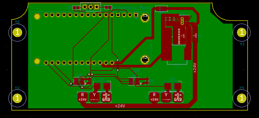
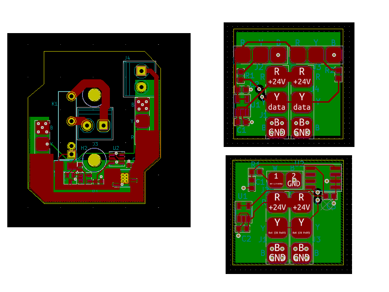
The experience has been excellent. Above all, the tool is very fast, efficient to use, and stable. Schematic and PCB integration works well enough, and routing and copper pours are easy. Switching between inches and millimeters can be done on the fly. The KiCad library has many parts in it, and other organizations, such as DigiKey, Seeed, SnapEDA, and Ultra Librarian are also providing libraries. If a KiCad symbol/footprint for a part is not already available, it is relatively easy to create new symbols and footprints as needed. There is a good KiCad support forum. KiCad is a pleasure to use and production-ready for standard PCB designs.
Read More »Reflections on KiCad and EDA Tools