(note, the article is also applicable to the i.MX6ULL as these processors are very similar)
The NXP i.MX6UL application processor has a very flexible pin multiplexer, that is somewhat difficult to understand at first glance. Most times when we’re configuring the pin mux in Linux, we modify Device Tree files, so perhaps that is the place to start. The pin mux options for the i.MX6UL are defined in the arch/arm/boot/dts/imx6ul-pinfunc.h file. The arguments to the macros in this file are defined as:
/*
 * The pin function ID is a tuple of
 * <mux_reg conf_reg input_reg mux_mode input_val>
 */
The first 5 are defined in the pinfunc.h file, where the config value is defined in a user’s DTS file. As an example, consider the following section from imx6ul-pinfunc.h. Column headings are added for clarity.
// headings:                                  mux_  conf_   input_ mux_ input
//                                            reg   reg     reg    val  _val
#define	MX6UL_PAD_GPIO1_IO09__PWM2_OUT        0x0080 0x030C 0x0000 0    0
#define	MX6UL_PAD_GPIO1_IO09__WDOG1_WDOG_ANY  0x0080 0x030C 0x0000 1    0
#define	MX6UL_PAD_GPIO1_IO09__SPDIF_IN        0x0080 0x030C 0x0618 2    0
#define	MX6UL_PAD_GPIO1_IO09__CSI_HSYNC       0x0080 0x030C 0x0524 3    1
#define	MX6UL_PAD_GPIO1_IO09__USDHC2_RESET_B  0x0080 0x030C 0x0000 4    0
#define	MX6UL_PAD_GPIO1_IO09__GPIO1_IO09      0x0080 0x030C 0x0000 5    0
#define	MX6UL_PAD_GPIO1_IO09__USDHC1_RESET_B  0x0080 0x030C 0x0000 6    0
#define	MX6UL_PAD_GPIO1_IO09__UART5_DCE_CTS   0x0080 0x030C 0x0000 8    0
#define	MX6UL_PAD_GPIO1_IO09__UART5_DTE_RTS   0x0080 0x030C 0x0640 8    2
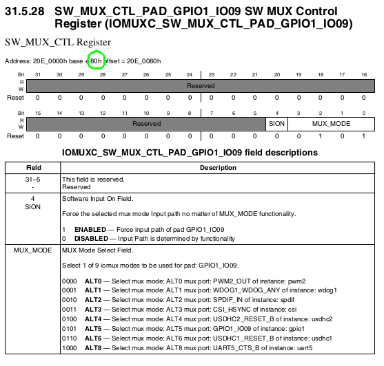
From the i.MX6UL processor reference manual (IOMUX Controller chapter), we can determine the mux_reg is indeed located at offset 0x80. We can also see that the mux_val values match MUX_MODE in the datasheet.
The mux_val in the imx6ul-pinfunc.h file also match the MUX_MODE field values in the above register.
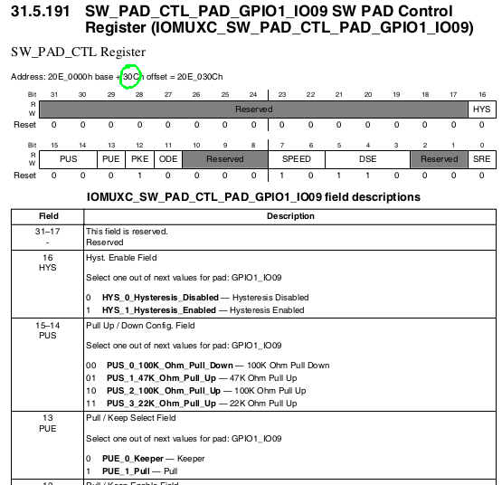
The config register can also be located in the datasheet. Again, we notice that the offset of 0x30C matches config_reg setting.
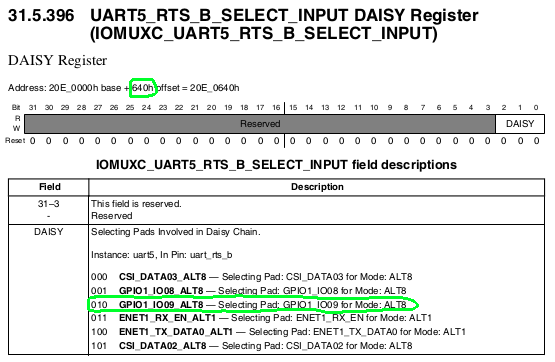
Lets consider the last option listed in the pinfunc file: UART5_DTE_RTS. The input register is used to mux a pin to an input function inside the SOC — in this case, the UART5_RTS_B input. We find the input register at offset 0x640 and can see that the input value of 0x2 matches what we would expect in the reference manual.
So, how do we know if the pinmux is configured correctly for a pin? One way is to use devmem2 and dump the register contents directly from user space:
root@imx6ul-var-dart:/sys/class/gpio# devmem2 0x20e0080
/dev/mem opened.
Memory mapped at address 0x76f02000.
Read at address  0x020E0080 (0x76f02080): 0x00000005
The mux value is 0x5, which configures the pin for the default GPIO1_9 function. Next we can look at the config register:
root@imx6ul-var-dart:/sys/class/gpio# devmem2 0x20e030C
/dev/mem opened.
Memory mapped at address 0x76f0b000.
Read at address  0x020E030C (0x76f0b30c): 0x000010B0
Bit index: 12─╮  8─╮  4─╮  0─╮
Bits:         1 0000 1011 0000
and can conclude that the following options are set:
- bits 3-5 = 6: DSE_43ohm
- bits 6-7 = 2: Medium speed (100MHz)
- bit 12: PKE: Pull/Keeper Enabled
There are additional options that can be configured such as hysteresis, pull up/down, open drain, and slew rate. I/O is very configurable on this device!
If we want to use this pin as a GPIO, it appears that everything is configured correctly, so let’s give it a try. GPIO in the i.MX6UL is banked in 32 bit registers, so we need to map this to a sequential GPIO in Linux. The formula for this mapping is:
linux gpio number = (gpio_bank – 1) * 32 + gpio_bit
For GPIO1_9, this would be GPIO9.
linux gpio number = (1 – 1) * 32 + 9 = 9
To read the GPIO, execute the following commands:
root@imx6ul-var-dart:~# cd /sys/class/gpio/
root@imx6ul-var-dart:~# echo 9 > export
root@imx6ul-var-dart:~# cat gpio9/value
0 (current gpio value)
Another nuance of configuring the i.MX6UL pin mux in Linux is that for GPIO outputs, you need to set a magical bit 30 in the Device Tree configuration as show below. If you don’t set bit 30, it will always read back as 0.
MX6UL_PAD_JTAG_TDO__GPIO1_IO12 0x4001b0b0 /* 2_nSLEEP */
The reason for this will be explored in a future post.


I did not know much about pinmux on iMX, this article helped me understand it and also enables to tweak it if needed.
Comments are closed.